Triple Bypass (3BP) — Mega Drive / Genesis
The reference AV mod for the Mega Drive: a daughterboard that bypasses the stock video stage and the stock audio stage — and, optionally, the 8-pin DIN of the Model 1. RGB and sound are tapped at the source, taken off the motherboard, and re-amplified cleanly.
Originally designed by db Electronics, it has become a genuinely open project: version 2 is a community redesign led by Tianfeng, with RetroRGB, Jose Cruz (testing), Ace, FirebrandX and Mobiusstriptech. The audio was tuned by ear and by measurement, using MDFourier by Artemio Urbina, to match the sound of a Model 1 VA3.
A mod for people who already solder
You will remove SMD components, lift IC pins and scrape solder mask off vias. This is not a first mod.
And above all: in nearly every case it disables composite video output. After this mod you need RGB / SCART cables, or cables that sync on composite (HD Retrovision). An ordinary composite cable will no longer produce a picture.
| Field | Value |
|---|---|
| Systems | Mega Drive / Genesis Model 1, Model 2, Model 3, Sega CDX |
| Type | video (RGB + csync) + audio bypass, plus the Model 1 DIN optionally |
| Level | 🔴 SMD removal, IC pin lifting — expert |
| Reversible | ❌ in practice: components removed, pins lifted |
| Design-file licence | CERN OHL v1.2 — the board can be made yourself |
Why this mod, concretely
Jailbars. All Genesis consoles output noisy analogue video, and these are some of the worst of the bunch. Simply lifting the subcarrier pin from the VDP already gives a noticeable reduction in jailbars on most Model 1 revisions — but it is not as good as a full bypass.
Moving the signals off the motherboard. All Genesis motherboards carry a good amount of interference in the audio and video signals. Tapping them at their sources and moving them off the board improves both a great deal. The circuits and components used in the Triple Bypass are equal to or better than what is on the board, with extra options: filtered or unfiltered sound at your choice, and a switchable low-pass filter on the video output.
What you gain per model:
- Model 1 — a big upgrade in video quality. The audio is already excellent; you gain a slightly quieter noise floor.
- Model 2 and 3 — decent but not good video, and audio that is poor or just mono. This is where the gain is most dramatic: Model 3s get genuinely excellent stereo, and Model 2s all sound excellent regardless of motherboard revision.
How the board works
Video
The board uses a THS7374 video amplifier. Depending on your model, you may need to lift the RGBS pins from the board, or add extra filtering capacitors.
⚠️ It outputs 75 Ω (not TTL) csync on the composite (CVBS) pin of the multi-out — but not actual composite video. That means that unless you use an alternate installation method (and risk adding interference back into the signal), composite cables no longer work, but anything that syncs on composite does, HD Retrovision cables included.
Audio
The board integrates the Mega Amp 2.0, originally designed by Ace, then tweaked using MDFourier measurements to reach levels matching the best version of the Model 1.
Signal reference — outputs, pass-throughs, inputs
This is the part that prevents installation mistakes: what each pad expects electrically, independent of revision.
Outputs
In a standard install these pins should be connected only to the output connector, with no other drivers or loads on them.
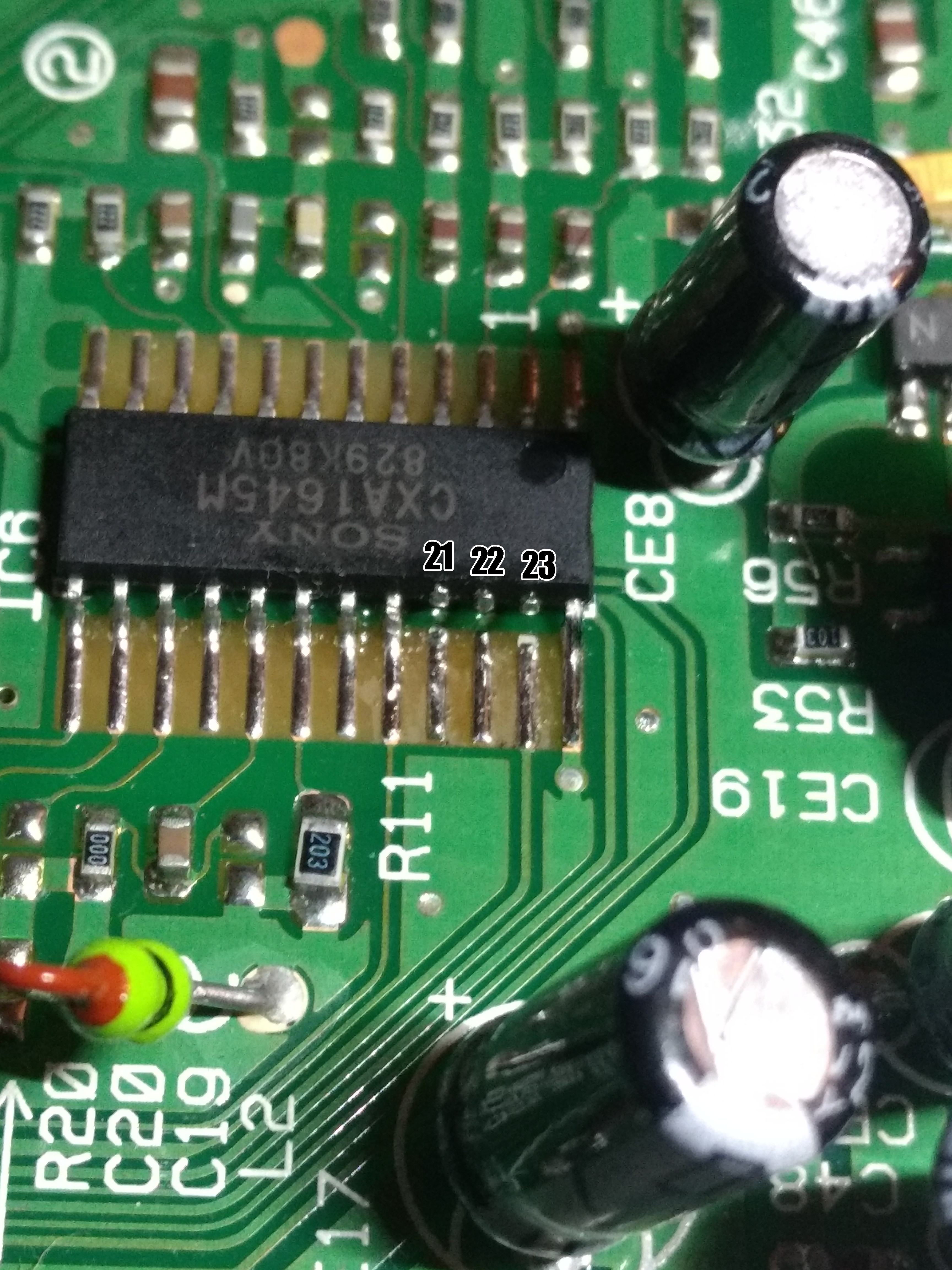
- Red, green and blue must no longer be connected to the video encoder. On all consoles these AV-port pins go directly to the encoder and nothing else. The connection is broken by lifting pins 21, 22 and 23 of the video encoder (⚠️ the pinout is the same for all revisions) or by cutting the traces to the port.
- Nothing on the mainboard should be loading the 3BP's driver for the composite pin (labelled "75" on the board). This is frequently omitted from existing guides. There is usually an AC coupling cap and an EMI filter or ferrite bead in series with this pin, which can be removed to separate it from the encoder (and, on Model 1, from the RF modulator). On later versions without an RF modulator you can also lift pin 20 of the encoder.
- The two stereo audio pins should not be driven by the existing circuitry on the main board. This is usually achieved by removing the output coupling capacitors as indicated in the Mega Amp install guides.
- The 3BP v2 does not drive the mono audio pin (unlabelled): no conflicts here. Typically this pin is not used by most 9-pin Mini-DIN cables — the major exception being the model 2/3 RF modulator (which will not work without composite anyway). If you are using the Model 1 8-pin DIN as your output and want mono audio, disconnect it from the encoder output in the same way as the composite pin.
Pass-throughs
Directly connected through, with no difference between the "input" and "output" pads.
- Composite sync (CSYNC) is used as an input only by the 3BP v2. The two pads labelled "S" are directly connected together, and the signal passes through unaltered if needed. On an install reusing the existing output port, typically only one need be connected. ⚠️ Many existing guides have you cut the CSYNC trace and jump a wire to the S pad — this is completely unnecessary. On a Model 2 bottom install, you need do nothing besides solder to the DIN pins.
- ⚠️ The 3BP v2 provides an extra pull-up resistor for CSYNC — this is R1. Ensure only one pull-up is connected to CSYNC: either remove R1 from the 3BP, or remove the stock pull-up from the mainboard if it is still in circuit.
- Ground is typically connected via the mini-DIN port itself. A ground pad is provided just in case but usually need not be used; the three large through-hole pads on the mini-DIN footprint are all ground.
- 5 volt power is typically present on the mini-DIN of Model 2 and 3. Unlike the other two, it can sometimes be beneficial to re-route it: disconnect the existing feed to the mini-DIN and run a wire directly from the 3BP to the voltage regulator.
Inputs
These are inputs to the board's amplifier circuits, with specific wiring requirements.
- Red, green and blue inputs should be connected with low impedance to the
corresponding output pins of the VDP (or ASIC, or GOAC).
- For the best picture quality, each of these signals should be connected by one 5.6 kΩ resistor to 5 V. ⚠️ Current versions of the 3BP v2 board do not have these resistors, so they must be provided externally. They are already present on the mainboard and the existing ones can be used (see the relevant revision below).
- In the stock circuit these signals reach the encoder network via a voltage divider and AC coupling capacitor. All of this should be disconnected, or the signal will be darker than intended. Usually, removing the 4.7 kΩ series resistor from each is all that is required.
- On some revisions it may be desirable to lift the RGB pins of the VDP/ASIC/GOAC and connect them directly to the 3BP. If this is done, the 5.6 kΩ resistors to 5 V must be added somewhere.
- XL/XR and CL/CR are electrically very similar.
- XL and XR connect to pins B01 and B03 of the cartridge slot. These audio inputs are fed by add-ons like the 32X or flashcarts (Mega Everdrive Pro, MegaSD).
- CL and CR connect to pins B29 and A29 of the expansion slot. They are fed by the Sega CD / Mega CD when the mixing jack is not used.
- For all four there are usually more convenient locations on the mainboard than the slots themselves (see the Mega Amp guides). These nets are fairly low impedance and not particularly vulnerable to noise.
- All four need one 75 Ω load/biasing resistor to ground. The jumpers on the 3BP v2 can connect its built-in 75 Ω resistors if there are none already in circuit.
- They should be disconnected from the existing audio circuit, usually by removing capacitors.
- YL/YR are the FM audio inputs, to be connected to the MOL and MOR pins of the FM
DAC (YM2612, ASIC or GOAC).
- On a board with a discrete YM2612 there should be 2.2 kΩ resistors to ground on each — typically already present.
- Nothing else should be connected to these pins (removing capacitors is typically enough).
-
PSG is the monaural signal from the integrated PSG/DCSG.
Your console has only one of the following chips, and whichever is present carries this signal on the pin labelled "PSG":
Chip Revisions Original VDP 315-5313 Model 1 before VA7 First integrated ASIC — 315-5487, 315-5660, 315-5700, 315-5708 (and -00, -01… variants) Model 1 VA7, several Model 2 revisions, Nomad Toshiba ASIC — 315-5685, 315-5786 Model 2 VA2 and VA2.3 First-iteration GOAC — 315-5960 Model 2 VA4, Genesis 3 VA1 Second-iteration GOAC — 315-6123 Genesis 3 VA2 - This signal always needs a pull-down/load/biasing resistor to ground. On most revisions this is 2.2 kΩ; on Toshiba ASIC revisions (Model 2 VA2 and VA2.3) 750 Ω is recommended. The 3BP v2 offers both via the "d" jumper.
- Your console likely already has one — but it may not be the correct value. Any wrong-value resistor should be removed, as well as any other load on the signal (capacitors, connections to the existing audio circuitry).
- ⚠️ If the correct value is already present, do not add a redundant one by soldering the "d" jumper. This is a mistake often made on early Model 2 boards: the instructions assume you removed the mainboard pull-down, and many people miss it.
Making the board yourself
The manufacturing files are archived here, under CERN OHL v1.2 — an open-hardware licence that explicitly permits reproduction and modification, provided the licence and notices are kept.
| File | Use |
|---|---|
| 📦 3BP v2.1 Gerbers (ZIP) | send as-is to a PCB fab |
| 📄 3BP v2 schematic (2022-05-17) (PDF) | understand, troubleshoot, modify |
| 📊 3BP v2 BOM (XLSX) | original bill of materials — transcribed below |
| 🛠️ 3BP v2.1 KiCad file | to modify the layout |
| ⚖️ CERN OHL v1.2 licence | keep with any copy |
| 📝 Repository README | the author's own version history |
What the author says about the KiCad files
The README is explicit and worth reading first: the board was designed in EasyEDA, and the KiCad file added in March 2020 is a re-draw. "It looks ok but I still see some issues with ground layers. I am new to kicad but this [is] pretty damn close. As it stands, I still recommend using the current gerber files to send to a pc[b] fab. The design files are good to go if you want to change or modify the design."
In practice: fabricate from the Gerber ZIP, use the KiCad only to modify.
Bill of materials — 3BP v2
Transcribed from the repository file, manufacturer part numbers included.
| Value | Designators | Footprint | Qty | Part | Manufacturer |
|---|---|---|---|---|---|
| 5.62 kΩ | R2, R3, R4, R5 | 0603 | 4 | RK73H1JTTD5621F | KOA Speer |
| 1.00 kΩ | R6, R7, R8, R9 | 0603 | 4 | RK73H1JTTD1001F | KOA Speer |
| 4.7 kΩ | R10 | 0603 | 1 | RK73H1JTTD4701F | KOA Speer |
| 75 Ω | R11, R13, R14, R17, R18 | 0603 | 4 ⚠️ | RK73H1JTTDD75R0F | KOA Speer |
| 2.20 kΩ | R1, R12, R15, R19 | 0603 | 4 | RK73H1JTTD2201F | KOA Speer |
| 750 Ω | R16 | 0603 | 1 | CR0603-FX-7500ELF | Bourns |
| 210 kΩ | R20, R21, R22, R23, R24, R25 | 0603 | 6 | RK73H1JTTD2103F | KOA Speer |
| 10 kΩ | R26, R27, R30, R33 | 0603 | 4 | RK73H1JTTD1002F | KOA Speer |
| 330 Ω | R36, R37 | 0603 | 2 | RK73H1JTTD3300F | KOA Speer |
| 300 kΩ | R34, R35 | 0603 | 2 | RK73H1JTTD3003F | KOA Speer |
| 100 kΩ | R29, R32 | 0603 | 2 | RK73H1JTTD1003F | KOA Speer |
| 130 kΩ | R28, R31 | 0603 | 2 | CR0603-FX-1303ELF | Bourns |
| 0.1 µF / 50 V | C1, C2, C3, C4, C5, C6, C20 | 0603 | 7 | C0603C104M5RACTU | KEMET |
| 22 µF / 10 V | C7 | 1210 | 1 | C3225X7R1A226K230AC | TDK |
| 220 µF / 6.3 V | C8 | tantalum, case B | 1 | TCOB0J227M8R-EN1 | ROHM |
| 1 µF / 16 V | C10, C11, C12, C13, C14, C15 | 0603 | 6 | C0603C105K4PACTU | KEMET |
| 10 µF / 10 V | C9, C16 | 0805 | 2 | EMK212BJ106KG-T | Taiyo Yuden |
| 150 pF / 50 V | C18, C19 | 0603 | 2 | CL10C151JB8NFNC | Samsung |
| 10 µF / 10 V | C17 | tantalum, case A | 1 | TAJA106K016RNJV | AVX |
| 47 µF / 10 V | C21, C22 | tantalum, case B | 2 | TAJB476M010TNJ | AVX |
| Op amp | U1 | SOIC-8 | 1 | TL972IDR | Texas Instruments |
| Video amp | U2 | TSSOP-14 | 1 | THS7374IPWR | Texas Instruments |
Two reservations, carried over as-is
⚠️ The 75 Ω line of the original BOM lists five designators (R11, R13, R14, R17, R18) but states a quantity of 4. The inconsistency is in the repository file: it is reproduced here rather than corrected, because there is no way to tell which of the two columns is right. Count the footprints on the Gerber before ordering.
⚠️ XL/XR mixing resistors — the ConsoleMods Model 3 VA1 page reports that these should be 300 kΩ rather than 210 kΩ. If you bought an assembled board and are getting volume-balance problems with Sega CD via a flashcart, this is the cause: replace with 300 kΩ, 0603, 1 % tolerance. The BOM above does say 210 kΩ at R20–R25 — that is what the original file says, and it is precisely what the note calls into question.
Jumper settings
Jumpers are set before fitting the board. They are silkscreened on the back of the 3BP, grouped by motherboard family.
| Boards | Jumpers to bridge | Source |
|---|---|---|
| Model 1 VA7 & Model 2 VA0 → VA1.8 | 2, C, D-right, E | the "M1va7 & M2va0-1.8" line silkscreened on the back of the board |
| Sega CDX | the "2" jumpers; plus d-right if you remove the PSG 2.2 kΩ | CDX guide |
The D jumper depends on a mainboard resistor
The instruction to solder D-right assumes R21 is not present on the mainboard. If it is present, leave the D jumper unconnected. This is an artifact of the original Mega Amp instructions telling you to remove it.
Model 2 VA4: a special case
Per Jose Cruz, the Model 2 VA4 has all the 75 Ω pull-downs on the Genesis mainboard. Nothing changes for the previous versions; just take note when installing in a VA4. (Silkscreen change of 2020-03-06.)
Installation by revision
Check your revision first
The revision is silkscreened on the motherboard (VA0, VA3, VA6.8…). The removal and tap points change from one revision to another: applying another revision's guide is how you tear a trace. No solder point here is inferred from a neighbouring revision.
State of the documentation available locally:
| Model | Revisions | Full guide here | Note |
|---|---|---|---|
| Model 1 | VA0 → VA7 | ❌ | See the note below |
| Model 2 | VA0, VA1, VA1.8 | ✅ | Bottom install recommended |
| Model 2 | VA2, VA2.3, VA3, VA4 | ❌ | Bottom install recommended except on VA4 |
| Model 3 | VA1 | ✅ | |
| Model 3 | VA2 | ✅ | |
| Sega CDX | — | ✅ | Composite restoration possible |
Model 1: what does not exist, and will not be invented
ConsoleMods hosts no illustrated guide for the Model 1: its VA3 page contains only a link to a written guide hosted on RetroRGB, and the VA0, VA1, VA2, VA4–VA7 pages are empty (red links). The repository README likewise points to RetroRGB for the RGB part and to the Sega-16 Mega Amp 2.0 thread for the audio.
So there is nothing to bring in-wiki: Model 1 solder points are in no freely redistributable source. Rather than invent plausible designators — which would have someone tear a trace — this page states what it does not have. The signal reference above holds for all revisions, and the post-installation fixes section carries the Model 1 preamp fix, which is fully documented.
Model 2 — VA0 (and, very likely, VA1 / VA1.8)
Guide transcribed from ConsoleMods (CC-BY-SA). It is given as 100 % supported for the VA0; the VA1 and VA1.8 are extremely similar in layout and may benefit extensively — it is your responsibility to verify that your board matches.
Tools: flush cutters, snips, soldering iron, solder, flux, solder wick, 28 or 30 AWG wire.
⚠️ After this mod, no more composite. You will need component (HD Retrovision) or RGB cables.
Opening up. Remove the 4 screws at the bottom, turn the console upright, lift off the top shell. Remove the screws on the metal shielding and lift the shield off. Remove the 2 screws on the sides of the cartridge slot. The motherboard now lifts out of the bottom shell.
Part 1 — prepping the top side
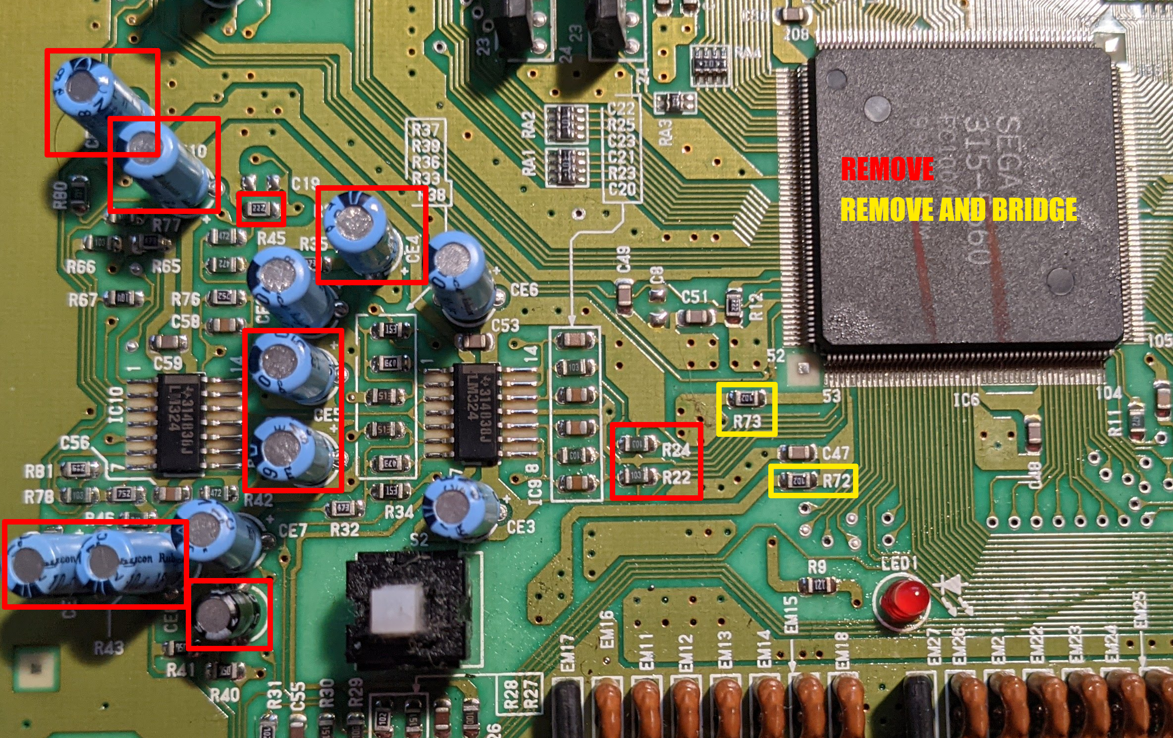
Box 1. Remove everything circled or boxed in RED. You can snip the capacitors with flush cutters, then use solder wick to remove the remaining solder and pull out the pins. Replace the items in PURPLE with solder bridges.
Once everything is removed and the bridges made, one thing remains in this area: connect the right side of R24 and the right side of R22 to the POSITIVE (+) through holes for CE5 and CE2 respectively. Push the wire through and solder on the bottom side (see Part 2, Box 1).
Box 2. Remove the single capacitor circled in RED.
Box 3.
- Lift the RGB pins on the video encoder: pins 21, 22 and 23. Heat the pin with your iron, then lift it away from the pad with a narrow tool. Make sure no solder links the pin to the pad.
- Remove R62, R63 and R64 — the RGB lines from IC6 to the video encoder. Removing them effectively cuts all current reaching the encoder along the RGB lines.
DO NOT remove R50, R51 and R52
These are required to remain in circuit. Otherwise you would have to install three 5.6 kΩ resistors independently.
Some guides and installers recommend removing the entire RGB circuit, but this is not entirely necessary. Lifting pins 21, 22 and 23 on the encoder and removing R62, R63 and R64 effectively disables the built-in RGB circuit. Leaving R50, R51 and R52 (the OEM 3 × 5.6 kΩ) in place eliminates the need to add the 5.6 kΩ resistors advised by RetroRGB and others. → Colour fix
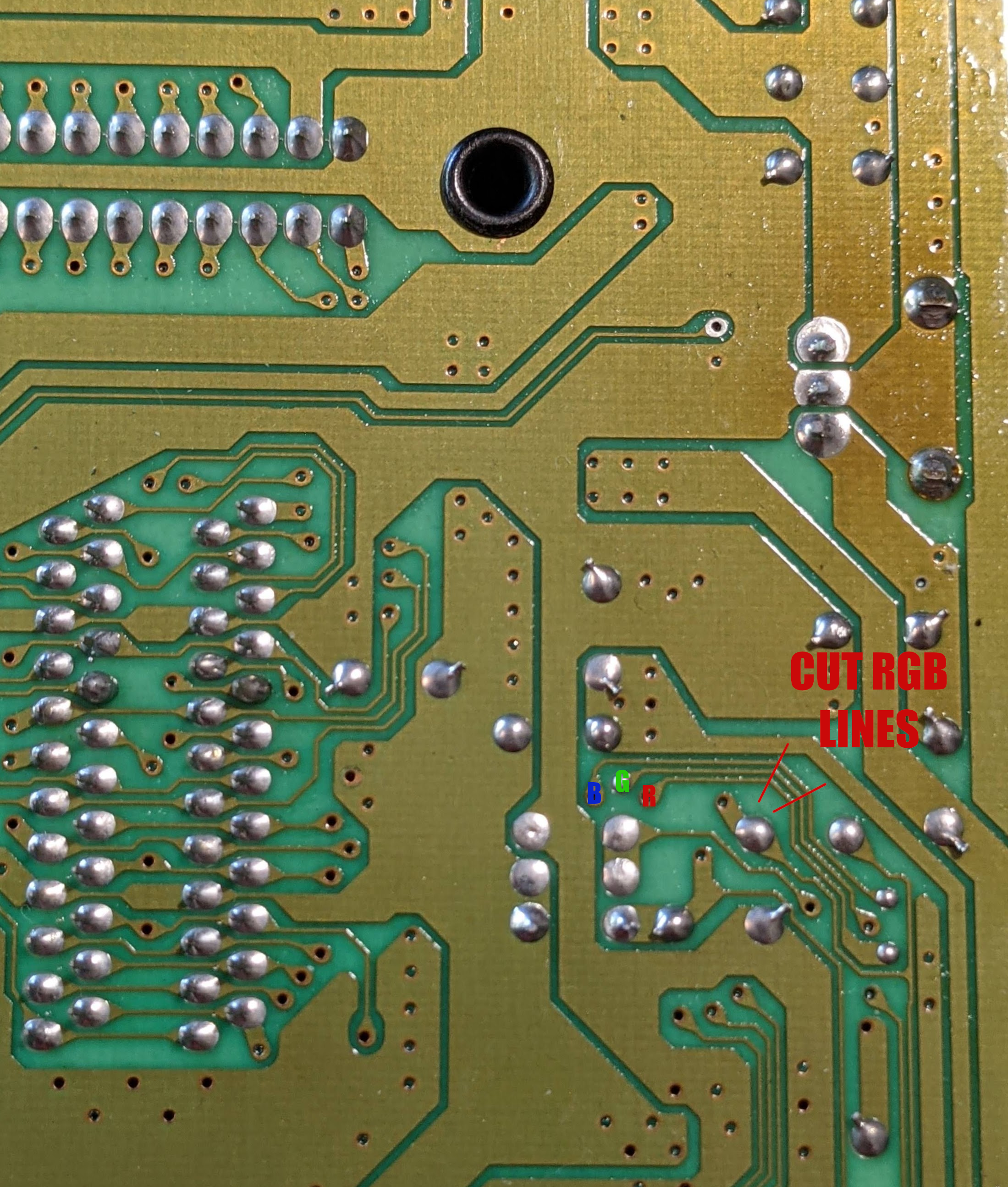
Box 4. Identify the three RGB vias used to connect the 3BP. They sit on the RGB lines, next to the label "L4". You can also follow the traces from R62, R63 and R64 towards the front of the board: three vias go to the bottom, run an inch or so, then come back up before running over to IC6.
Part 2 — prepping the bottom side
Box 1.
- Tin each of the through holes circled in RED (the former capacitors) with a small bit of solder.
- Add additional solder to the 5 V pin.
- Scrape the solder mask off the CSYNC via to expose shiny copper. ⚠️ Do not scrape too hard or too much — you do not want to damage the copper. Tin lightly.
- Do the same for the three RGB vias. Tin lightly.
DO NOT cut or damage the RGB traces anywhere from IC6 to R50, R51 and R52
It is important to keep these resistors in circuit.
Box 2.
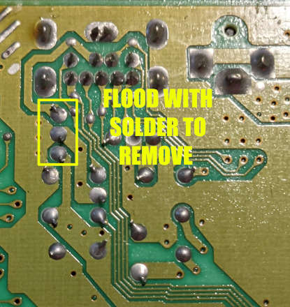
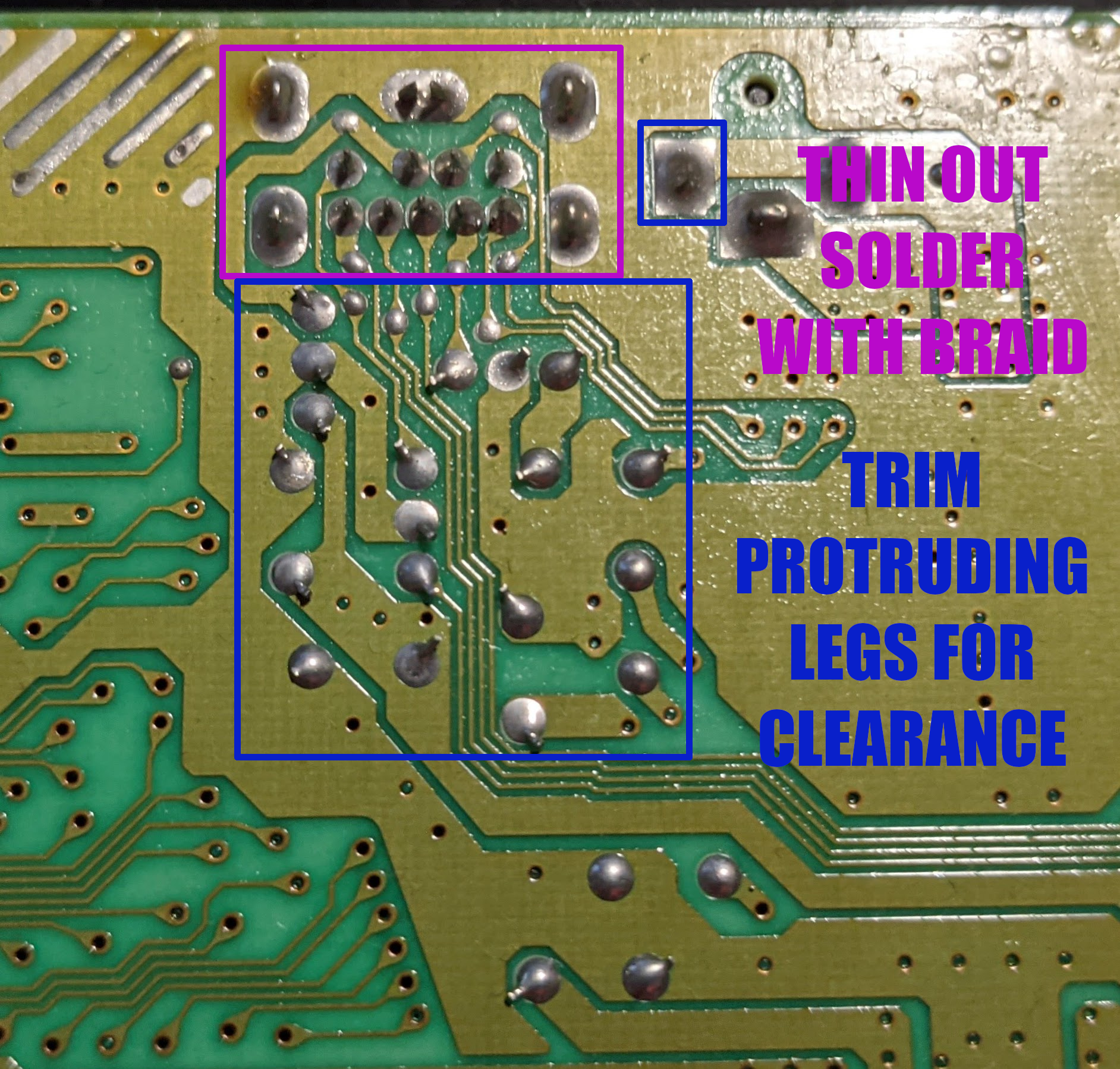
- The pins circled in RED at the DIN port are too long for the 3BP to sit flush against the motherboard. They must be trimmed. The power-port pins also need securing.
- Remove the solder from each pin circled in RED with solder wick, then trim them flush to the board with flush cutters.
- Once trimmed, add a small amount of solder back to re-secure them.
- Reflow / re-solder the 2 pins circled in BLUE: these often crack over time on these models. Do it now, while you are there.
Part 3 — prepping the 3BP board
Set the jumpers (see Jumper settings): on the back of the 3BP, under the line reading "M1va7 & M2va0-1.8", bridge 2, C, D-right and E.
Then tin all the inputs on the bottom and right edges of the 3BP: YR, CR, XR, PSG, XL, CL, YL, 5V, S (CSYNC), R, G, B.
Fitting on the DIN. Line up the output through holes (top of the board) with the DIN pins: the 3 large holes line up with the 3 upper-most pins, the rest follow. There is only one way the 3BP will sit. Solder the 3 large holes first to secure it in position. Then add generous flux to the smaller holes and solder each with just enough solder to make contact with the pin beneath.
⚠️ Do not use too much — bridged adjacent holes are easy to miss. Use a multimeter to check there is no continuity between any two adjacent holes.
Part 4 — solder all connections
Connect each 3BP input to its corresponding source on the board: YR on the 3BP to the source labelled YR on the bottom of the board, CR to CR, PSG to PSG, and so on.
⚠️ Route the wires clear of the slot pins. When the board goes back in the shell, a small plastic bracket sits under the slot: if the wires run there, the console will not go back together.
Part 5 — bottom shield plate modification
Even sitting flush, the 3BP is still too thick to fit with the metal shield in place. You can remove the shield, but this is not recommended: it protects the rest of the board from static and dust. Simply trim the shield with snips enough to clear the 3BP.
Then reassemble the console.
Plates — Model 2 VA0
These plates come from the 3BP v2 repository (Install/VA0VA1.8 folder, CERN OHL v1.2)
and not from ConsoleMods, whose image set for this revision could not be archived. Their
colour code is therefore red = remove / yellow = remove and bridge, where the ConsoleMods
text above says "purple" for bridges. It is the same operation.
MSVA0 in the
repository, where its four siblings are named M2VA0 — the author does
not explain the discrepancy. Compare against your own board before cutting anything.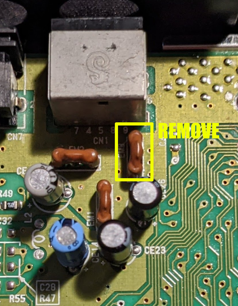
Model 3 — VA1
Guide transcribed from ConsoleMods (CC-BY-SA).
Tools: flush cutters, snips, iron, solder, flux, wick, 28 or 30 AWG wire.
⚠️ After this mod, no more composite: RGB or HD Retrovision cables required.
Opening up. 4 screws underneath, top shell, shield screws, shield, 2 screws either side of the cartridge slot, then the board lifts out.
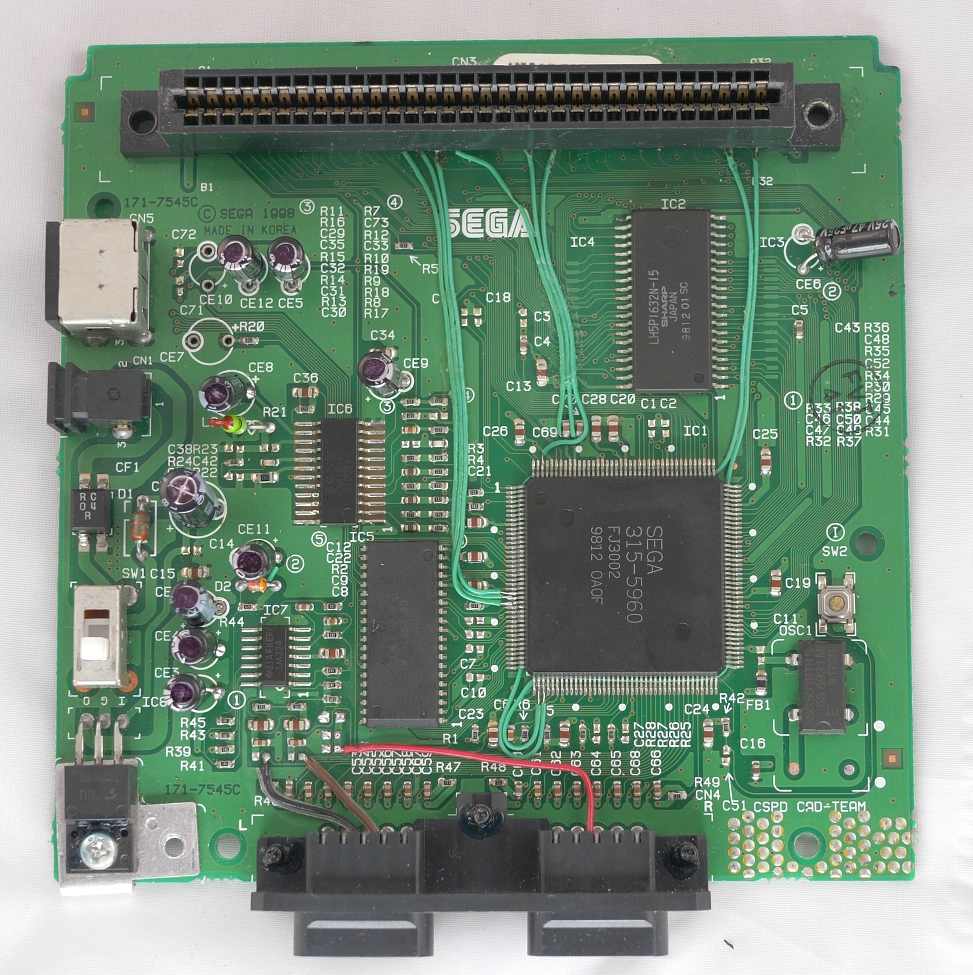
- Cut the trace indicated and verify with a multimeter that there is no continuity between the two points.
- Mount the bypass board on the top of the motherboard. The recommended spot is on the right-hand side, on the large solder joints sticking up.
- In that spot, the 3BP blocks the hole for a plastic standoff on the shell. Completely remove that standoff by trimming it with flush cutters.
- Lift the RGB pins — 21, 22 and 23 — from the CXA1645M chip.
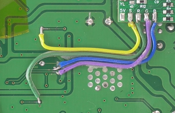
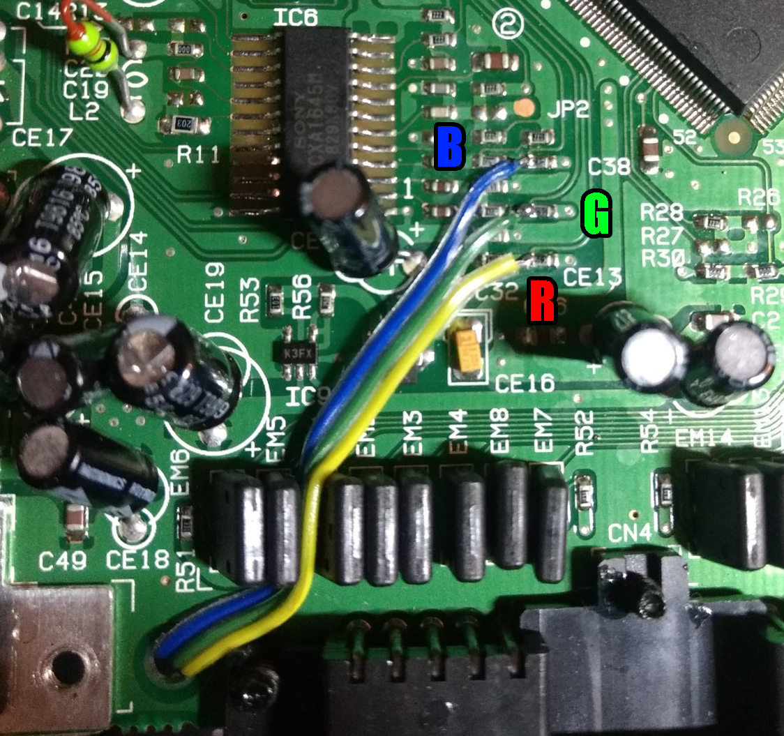
- Solder wires from the video signal (RGBS) pads on the bypass board to the vias indicated.
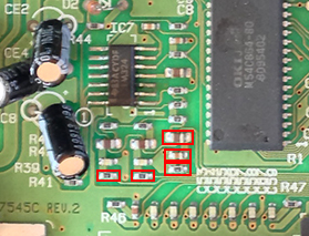
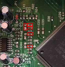
- Remove the five components indicated. Also remove the electrolytic CE10 (mono output capacitor) and CE7 (composite video output) near the mini-DIN connector.
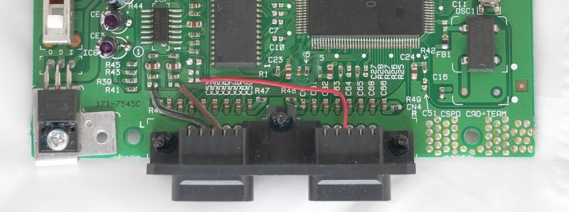
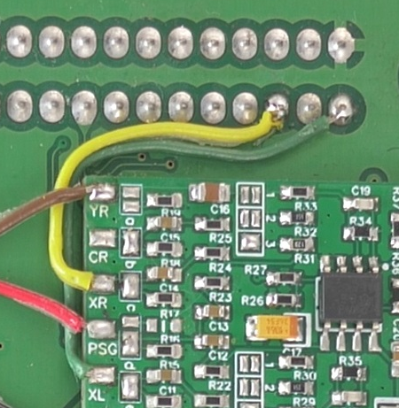
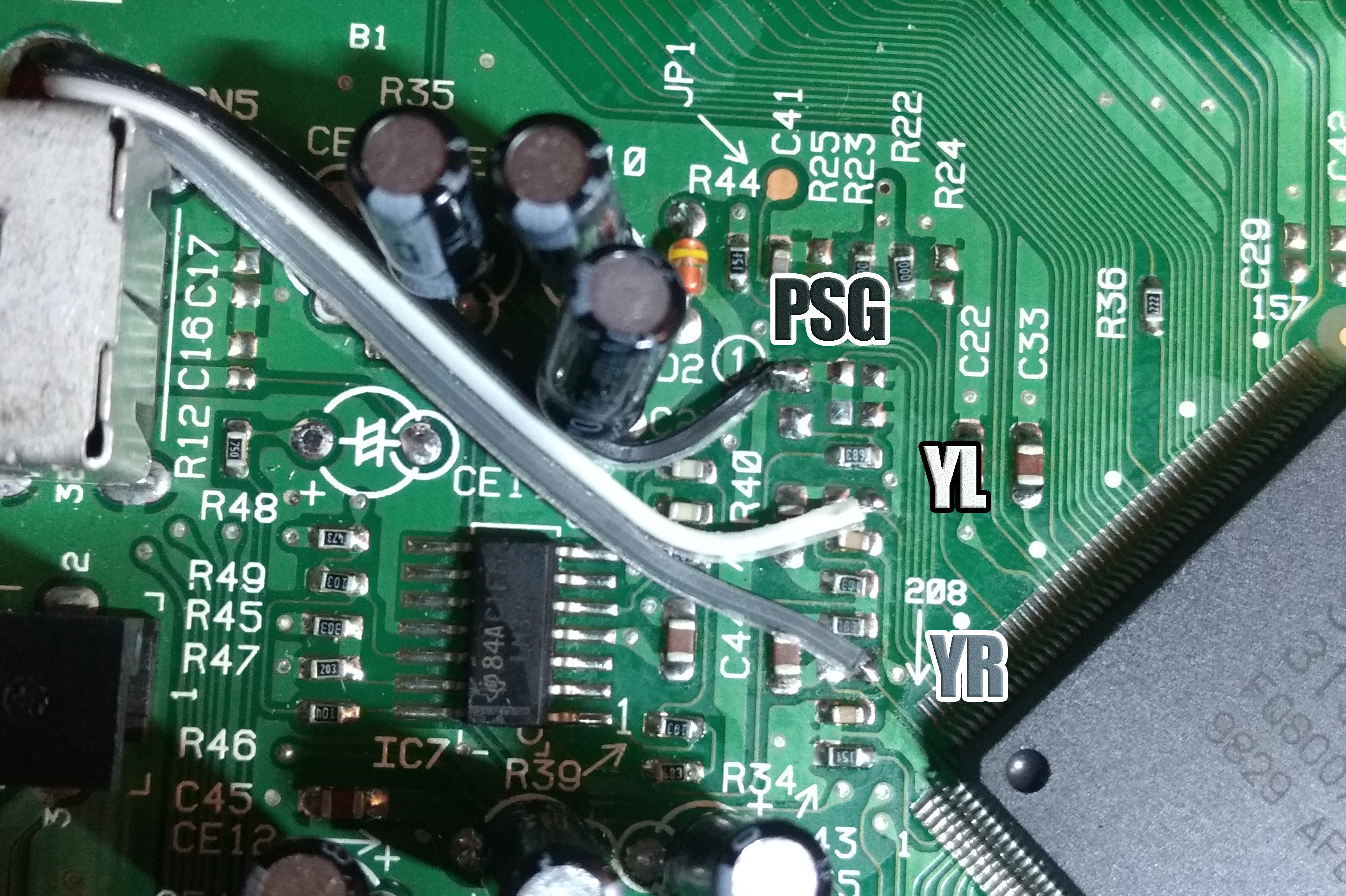
- Solder wires from the audio (YL / YR / PSG) pads to the resistors indicated on the bottom side, snaking the wires through the controller ports to the top side.
- Solder wires from the XL / XR pads to cartridge connector pins B1 (XL) and B3 (XR).
XL/XR mixing resistors — 300 kΩ, not 210 kΩ
It has been discovered that the XL/XR mixing resistors should be 300 kΩ. If you bought your board and are getting volume-balance issues with Sega CD via a flashcart, this is the cause. Replacements: 300 kΩ, 0603, 1 % tolerance.
Model 3 — VA2
Guide transcribed from ConsoleMods (CC-BY-SA). Same tools, same warnings, same opening procedure as the VA1.
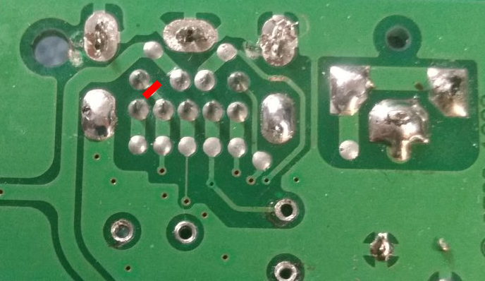
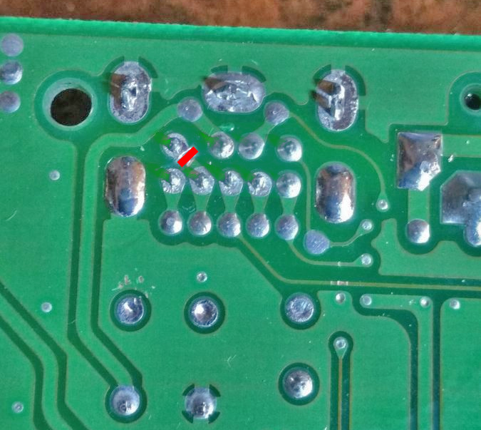
- Cut the trace indicated and verify with a multimeter that continuity is gone. This trace connects the mono audio pin and the stereo left channel together.
- Mount the board on top, on the right-hand side, on the large solder joints sticking up.
- Completely remove the plastic standoff that the 3BP blocks.
- Lift the RGB pins — 21, 22 and 23 — from the CXA1645M chip.
- Remove the five components indicated: these are the left channel, right channel and PSG inputs of the original audio circuit. Also remove the electrolytic CE7 (mono audio output). ⚠️ Failure to remove CE7 will cause the left audio channel to be a lower volume.
- Solder three wires from the points indicated to the corresponding ones on the 3BP.
- Remove the components indicated and solder three wires to the Red, Green and Blue pads, running them through the hole near the edge of the board to the 3BP. Also remove the electrolytic CE11, which disconnects the composite video output.
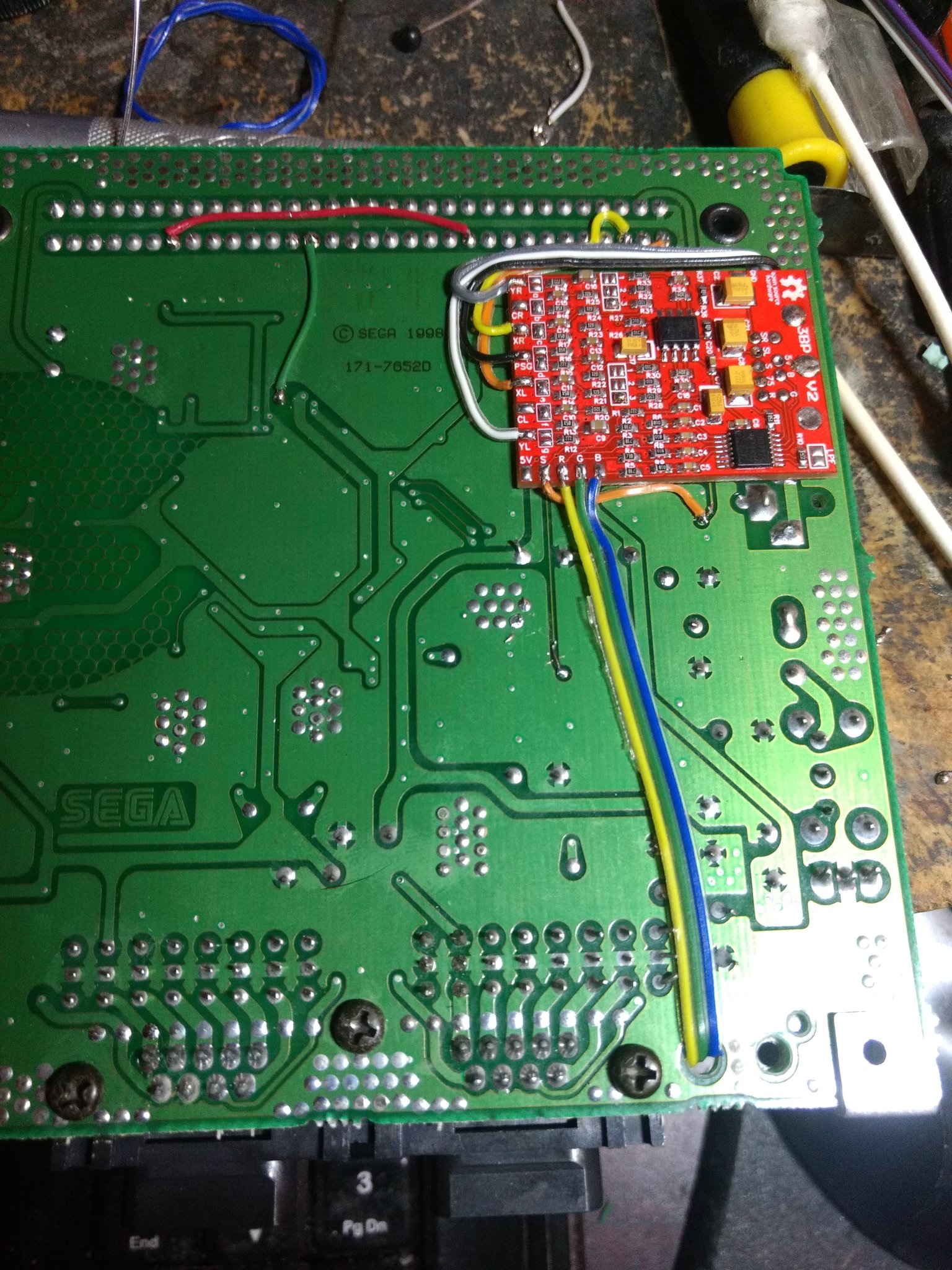
Sega CDX
Guide transcribed from ConsoleMods (CC-BY-SA). The CDX is the only install on this page where composite can be restored — at the cost of a few extra components.
Jumper settings
- Solder the "2" jumpers.
- If removing the 2.2 kΩ PSG resistor (below), also solder the d-right jumper.
Top-side component removal
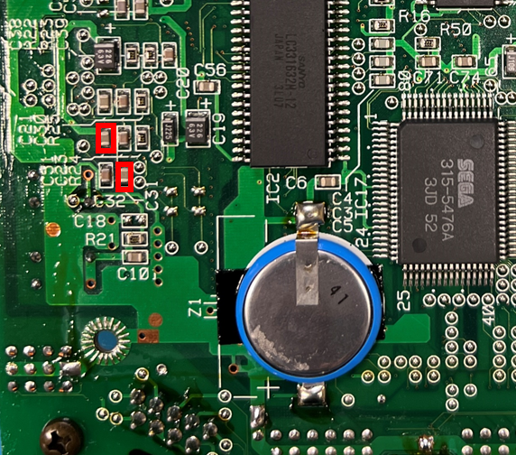
FML, 32X, PSG. Remove the components boxed in red. R81 is optional, but removing it makes connecting PSG easier — ⚠️ if you do, solder the d-right jumper.
RGB output. Remove the components boxed in red. The components in yellow must be removed only if composite restoration is not desired.
CDX revisions
Some CDX revisions have traces connecting the pads of the jumper. If so, either cut the trace between the pads, or lift encoder pins 21–23.
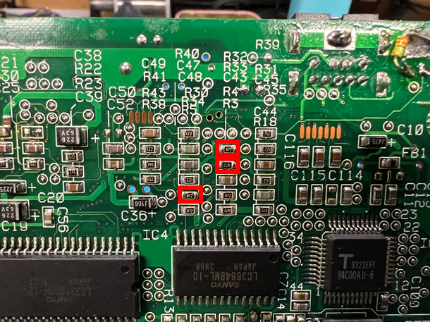
Cart to CD/PCM audio mixing. Remove the components shown in red, and replace R75 and R76 with 4.7 kΩ resistors, 0603 or 0805, 1/8 W or better.
Bottom-side component removal
- FMR and PSG AC coupling capacitors: remove the components boxed in red.
- RGB encoder input resistors: remove those indicated.
Installation
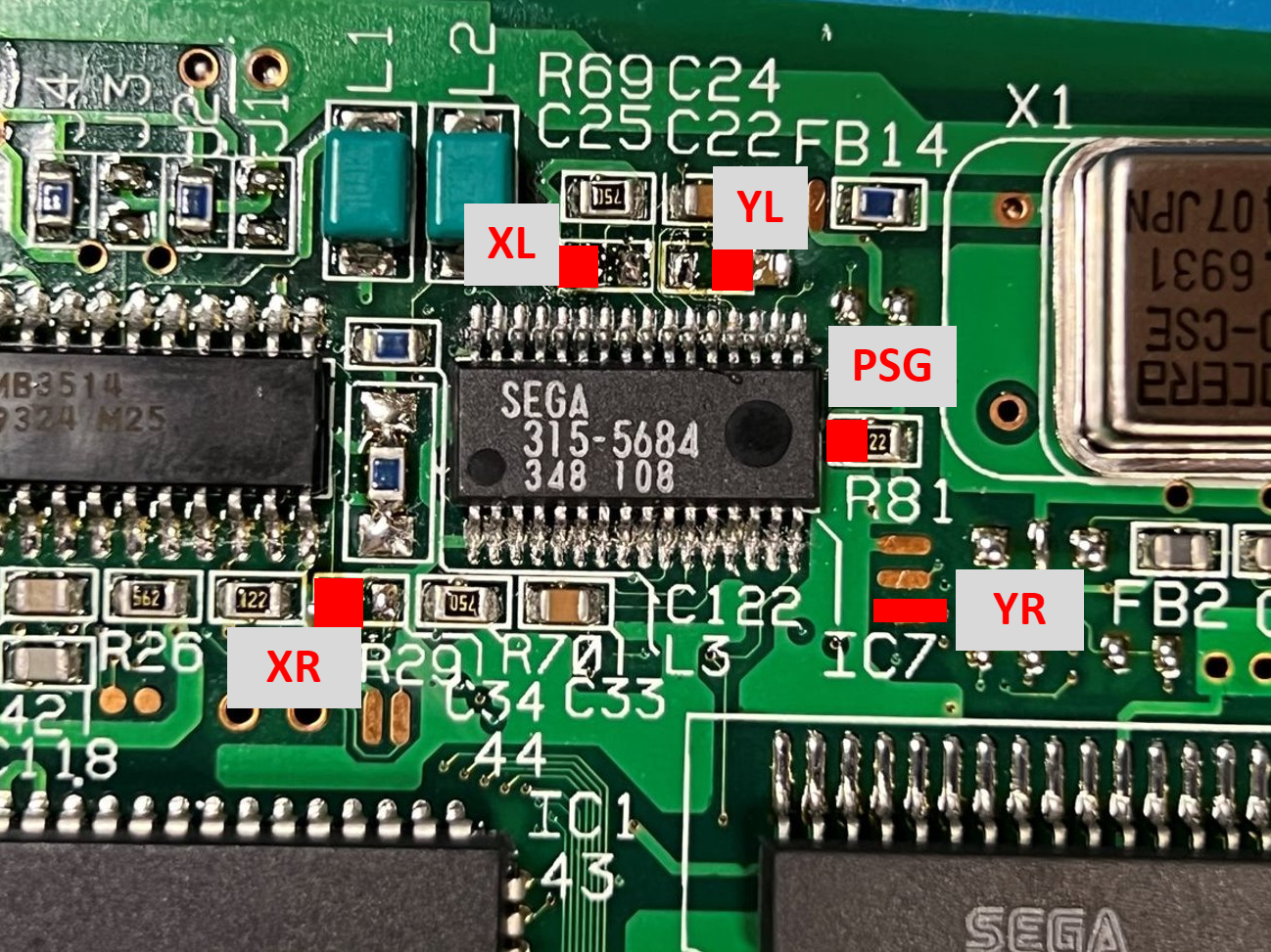
- Audio inputs — connect the 3BP audio input pads to the points labelled. ⚠️ There is NO input for "CL" or "CR" on this machine.
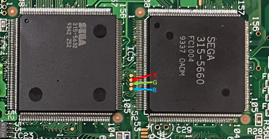
- RGB inputs — connect the 3BP RGB input pads to the points labelled. For TTL sync, refer to the component-removal image above if composite restoration is not desired.
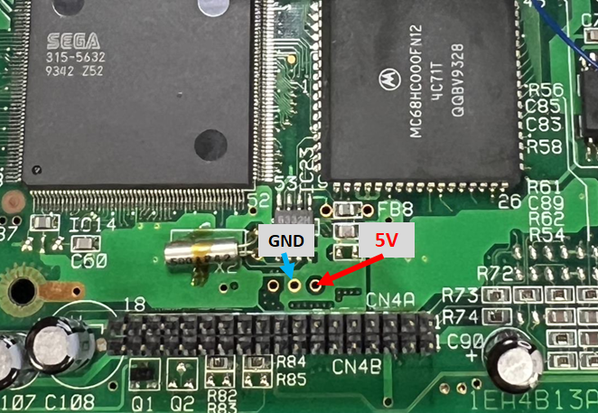
- 5 V and GND — suggested connection points; others may also be suitable.
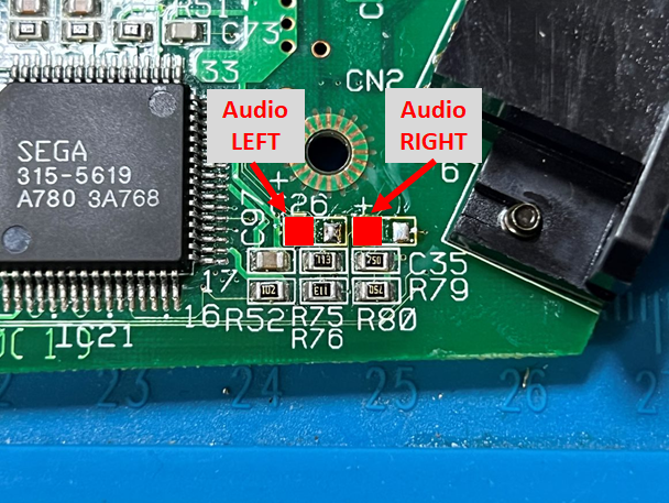
- Audio outputs — connect the 3BP left and right audio outputs to the points shown.
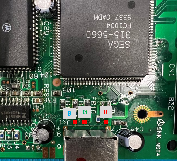
- RGB video outputs — as shown. If not restoring CVBS, connect the "S75" output pin to the through hole for C46(−). The installation is then finished.
Composite (CVBS) restoration — optional
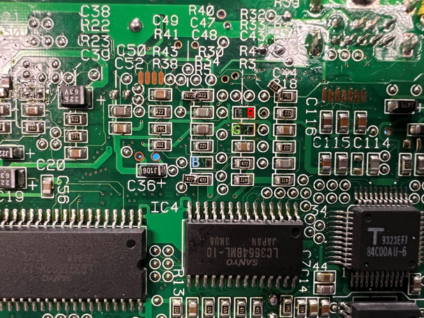
Use the points indicated. The 3BP V2Plus has 511 Ω resistors connected to the "R0", "G0" and "B0" pads. Otherwise use a value between 470 and 511 Ω to connect the RGB output to the pads indicated.
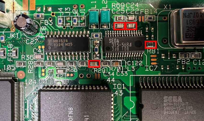
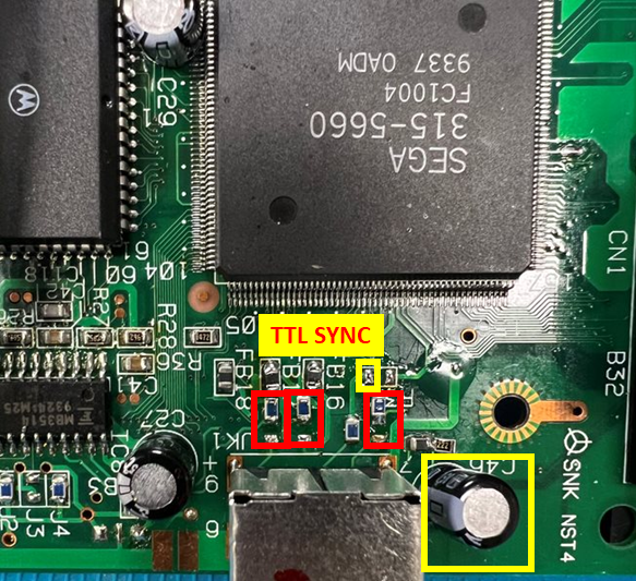
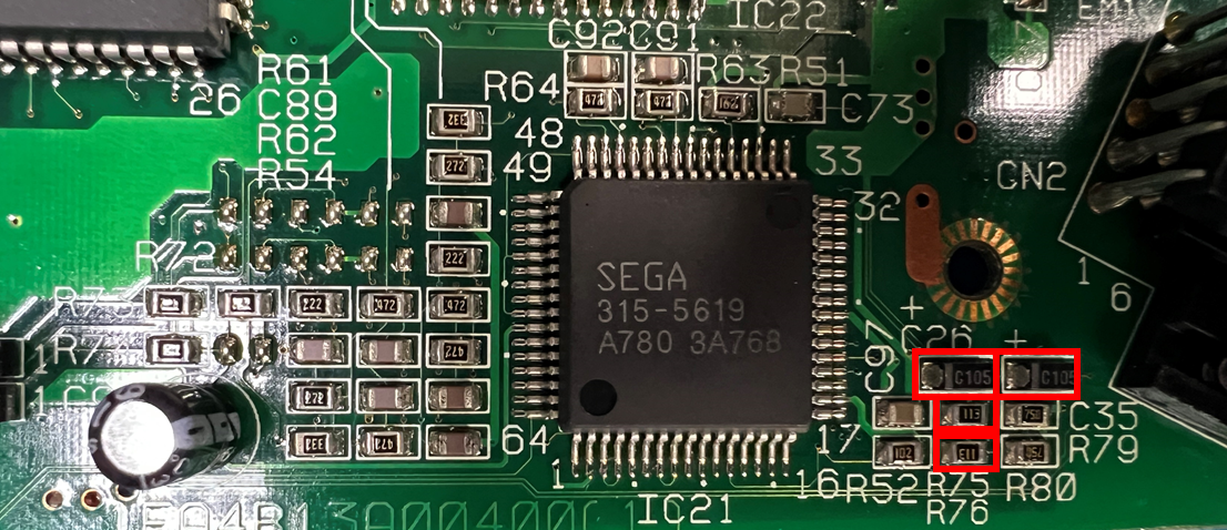
Post-installation fixes
Colour fix after an RGB bypass
Documented by Tianfeng. If you used a regular bypass board — one that does not fully replicate the original circuit — and you lifted the RGB pins, the colours will be slightly incorrect.
Fix: add a 5.6 kΩ resistor (three in total) from each of the R, G and B pads on the board to a 5 V pad on the motherboard.
This is exactly what the Model 2 VA0 procedure avoids by keeping R50, R51 and R52.
Preamp fix — Model 1 only
Early Japanese Model 1 Mega Drives and the earliest US Genesis consoles have slightly overdriven audio from the headphone jack, slightly spoiling what is otherwise well-balanced and clean stereo output. Sega corrected this from the VA3 revision onwards; on VA0 through VA2 it can be corrected by substituting several component values.
This modification was originally developed by Ace on the Sega-16 forums. It is also the only audio modification approved by the 16-bit Audiophile Project for recording high-quality Genesis/Mega Drive game soundtracks.
⚠️ This mod greatly reduces the volume of the mono output (AV out and RF). It can be restored, through the heavier modification of procedure 2.
Materials and tools
- JIS/Phillips screwdriver
- Soldering iron, leaded solder, flux, tweezers
- Two 10 kΩ 1206 SMD resistors
- One 18 kΩ 1206 SMD resistor
- Two 4700 pF 1206 SMD capacitors
- One 33 kΩ SMD resistor
- Some 28 AWG wire
- Optional: one TL972 op amp or similar
Procedure 1 — preamp fix. The points differ by board: VA0, VA1 and Japanese VA2 on one hand (the points are the same for all three), US VA2 on the other.
Those particular points are not transcribed here
ConsoleMods documents this step through annotated photographs only, with no list of designators in the text. Those images could not be archived locally, and inventing plausible references would have someone desolder the wrong component. → Preamp Fix (Model 1) on ConsoleMods
Procedure 2 — mono fix (optional, US VA2). This one is spelled out in words at the source, so it is reproduced here:
- Remove the 8-pin LM358 op amp from the motherboard. It is located between the Yamaha YM2612 and the Sony CXA1145 video encoder.
- Cut the traces connecting pins 1 and 2 of the op amp to the negative leg of capacitor C30, then cut the trace joining pins 1 and 2. Test with a multimeter to ensure conductivity is lost.
- Cut the trace going from pin 3 on the topside. If you wish to keep all wiring on the topside, sever down the middle so as to allow step 4.
- Connect pin 1 on the motherboard to the negative leg of C30, then connect the trace originally going to pin 3 to pin 2 instead. This can be done from the top or bottom side.
- After reinstalling the original op amp (or a socket in its place), solder a 33 kΩ resistor between pins 1 and 2 of the op amp. Optional: keep the original op amp, or replace it with a more modern one such as a TL972. If undecided, install a socket to make future upgrades easier.
- Solder a wire from pin 3 of the op amp to pin 5 of the Sony A1034 headphone amp.
- Hook the system up to test, and enjoy.
Sega CD audio with a flashcart
If you use a Mega SD or Mega EverDrive PRO, Sega CD audio is easily restored — this is what the green wires on the Model 3 photographs above are. → Sega CD Audio on ConsoleMods.
Where to buy
- Bare board: make it from the Gerbers archived here.
- Assembled boards: Insurrection Industries, RetroGamerStuff.
- Variants: versions exist for the Master System, the Nomad and others, made by community members. A Zaxour remix also exists (the RGB-pin-lifting caveats do not apply to it in the same way).
- Model 2 DIN adapter: a shared project on OSH Park (Model 2 DIN Breakout).
Alternatives / companions
- Region-free Mega Drive (language + 50/60 Hz): see Region-free.
- ODE / flashcart: Mega SD.
- SCART wiring: RGB & SCART.
- Console page: Mega Drive.
Sources & attribution
Manufacturing files (archived in this wiki):
- Tianfeng et al. — Triple Bypass Version 2: Gerbers, schematic, BOM, KiCad, README — CERN OHL v1.2 (archived licence) — https://github.com/tianfeng33/triple-bypass-Version-2
- Original design: db Electronics. v2 redesign: Tianfeng, with RetroRGB, Jose Cruz (testing), Ace, FirebrandX, Mobiusstriptech. Audio tuning with MDFourier (Artemio Urbina), with Bfbii.
- Mega Amp 2.0 — designed by Ace (Sega-16 forums), integrated into the 3BP.
Procedures and plates:
- ConsoleMods — Genesis: Triple Bypass Mod — CC-BY-SA — https://consolemods.org/wiki/Genesis:Triple_Bypass_Mod
- ConsoleMods — Genesis: Triple Bypass Mod Technical Details (signal reference) — CC-BY-SA
- ConsoleMods — Model 2 VA0, Model 3 VA1, Model 3 VA2, Sega CDX guides — CC-BY-SA — transcribed and illustrated here
- ConsoleMods — Genesis: RGB Bypass Color Fix (after Tianfeng) — CC-BY-SA
- ConsoleMods — Genesis: Preamp Fix (Model 1) (after Ace, Sega-16) — CC-BY-SA
- Model 2 VA0 plates:
Install/VA0VA1.8folder of the 3BP v2 repository — CERN OHL v1.2
Not carried over, and why:
- Model 1 solder points: ConsoleMods hosts none (the VA3 page is a bare outbound link; VA0/VA1/VA2/VA4–VA7 are empty). The repository points to RetroRGB for RGB and to the Sega-16 Mega Amp 2.0 thread for audio. Nothing is inferred from a neighbouring revision.
- The Model 1 preamp-fix annotated photographs: not archivable, and not replaceable by a description.
- The ConsoleMods Model 2 VA0 image set: absent from the public archives. Replaced by the repository's plates, under a free licence.
Review & corrections
How this space is used
Spotted a wrong value, an outdated procedure, a chip reference that does not match your board? Say so here, with what you observed (model, board revision, serial number, measurement). Every report is cross-checked against a source before anything changes — an unverifiable correction is published as “reported by …, not cross-checked” rather than silently applied.
Reading is open to everyone; posting requires signing in with Discord. Reports from the wiki's declared reviewers are handled first; anyone else's are read too, but go through a human before anything is changed.